
ATE Articles

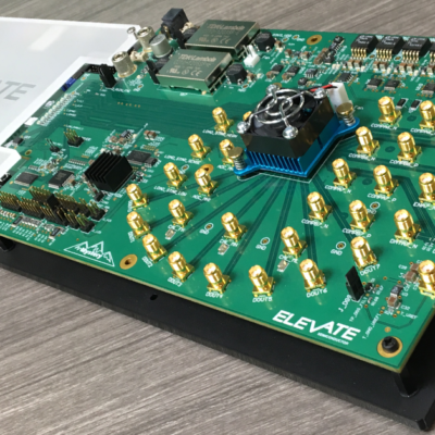
January 30, 2024
Elevate Semiconductor offers a diverse array of products, and the Evaluation Module (EVM) plays a pivotal role in the assessment…
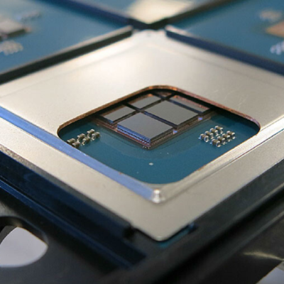
December 13, 2023
Tackling Complex Challenges in Semiconductor Chiplet Testing In semiconductor technology, chiplets have emerged as modular components that can operate either…

October 30, 2023
Interview with Anthony Turvey, Director of High Speed IC Design at ElevATE Interviewer: How did you end up in the…
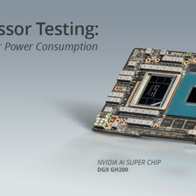
September 18, 2023
AI Processors, such as prominent models like Graphcore and NVIDIA’s AI Super Chip GH200, demonstrate formidable computational power. With power…
July 27, 2023
By Simon Leigh, Elevate VP of Engineering As the intricacy of testing grows, it’s essential for ATE vendors to continually…
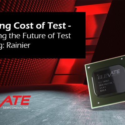
April 9, 2023
ACING THE TEST: THE CHIPS BEHIND THE CHIPS. ENGINEERING.COM The crucial ATE industry has never faced more challenges—but companies like…
January 22, 2022
ATE digital systems traditionally consist of sequencers, formatters, timing generators and pin electronics. The decision about which components to use for…
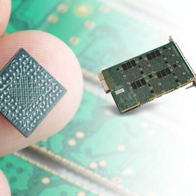
May 4, 2021
Typical integrated circuit (IC) solutions for pin electronics (PE) have been provided by multiple semiconductor companies in multiple different process…
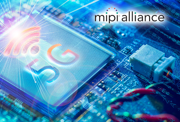
November 15, 2020
MIPI Specifications and Testing ATE Articles / By admin The mobile industry processor interface (MIPI®) standard defines industry specifications for the design…
June 12, 2020
As technology evolves, and demand increases for next generation chips in artificial intelligence, deep learning, machine learning, automotive, IOT, healthcare…
March 2, 2020
Device Power Supplies (DPS) semiconductors provide flexible voltage and current force measurement capabilities to meet a wide range of test…

April 1, 2019
ELEVATE: WORLD LEADER IN INTEGRATED TEST TECHNOLOGY THE BASICS OF SEMICONDUCTOR TEST:Technology aficionados know Moore’s Law which states the number…